The Scientist and Engineer's Guide to
Digital Signal Processing
By Steven W. Smith, Ph.D.
Book Search

Table of contents
- 1: The Breadth and Depth of DSP
- 2: Statistics, Probability and Noise
- 3: ADC and DAC
- 4: DSP Software
- 5: Linear Systems
- 6: Convolution
- 7: Properties of Convolution
- 8: The Discrete Fourier Transform
- 9: Applications of the DFT
- 10: Fourier Transform Properties
- 11: Fourier Transform Pairs
- 12: The Fast Fourier Transform
- 13: Continuous Signal Processing
- 14: Introduction to Digital Filters
- 15: Moving Average Filters
- 16: Windowed-Sinc Filters
- 17: Custom Filters
- 18: FFT Convolution
- 19: Recursive Filters
- 20: Chebyshev Filters
- 21: Filter Comparison
- 22: Audio Processing
- 23: Image Formation & Display
- 24: Linear Image Processing
- 25: Special Imaging Techniques
- 26: Neural Networks (and more!)
- 27: Data Compression
- 28: Digital Signal Processors
- 29: Getting Started with DSPs
- 30: Complex Numbers
- 31: The Complex Fourier Transform
- 32: The Laplace Transform
- 33: The z-Transform
- 34: Explaining Benford's Law
How to order your own hardcover copy
Wouldn't you rather have a bound book instead of 640 loose pages?Your laser printer will thank you!
Order from Amazon.com.
Chapter 3: ADC and DAC
A popular technique in telecommunications and high fidelity music reproduction is single bit ADC and DAC. These are multirate techniques where a higher sampling rate is traded for a lower number of bits. In the extreme, only a single bit is needed for each sample. While there are many different circuit configurations, most are based on the use of delta modulation. Three example circuits will be presented to give you a flavor of the field. All of these circuits are implemented in IC's, so don't worry where all of the individual transistors and op amps should go. No one is going to ask you to build one of these circuits from basic components.
Figure 3-16 shows the block diagram of a typical delta modulator. The analog input is a voice signal with an amplitude of a few volts, while the output signal is a stream of digital ones and zeros. A comparator decides which has the greater voltage, the incoming analog signal, or the voltage stored on the capacitor. This decision, in the form of a digital one or zero, is applied to the input of the latch. At each clock pulse, typically at a few hundred kilohertz, the latch transfers whatever digital state appears on its
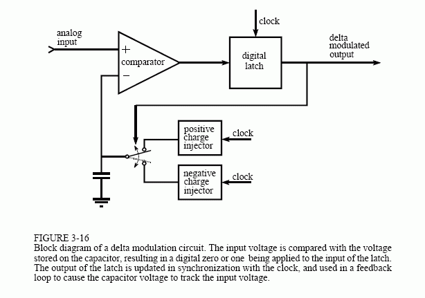
input, to its output. This latch insures that the output is synchronized with the clock, thereby defining the sampling rate, i.e., the rate at which the 1 bit output can update itself.
A feedback loop is formed by taking the digital output and using it to drive an electronic switch. If the output is a digital one, the switch connects the capacitor to a positive charge injector. This is a very loose term for a circuit that increases the voltage on the capacitor by a fixed amount, say 1 millivolt per clock cycle. This may be nothing more than a resistor connected to a large positive voltage. If the output is a digital zero, the switch is connected to a negative charge injector. This decreases the voltage on the capacitor by the same fixed amount.
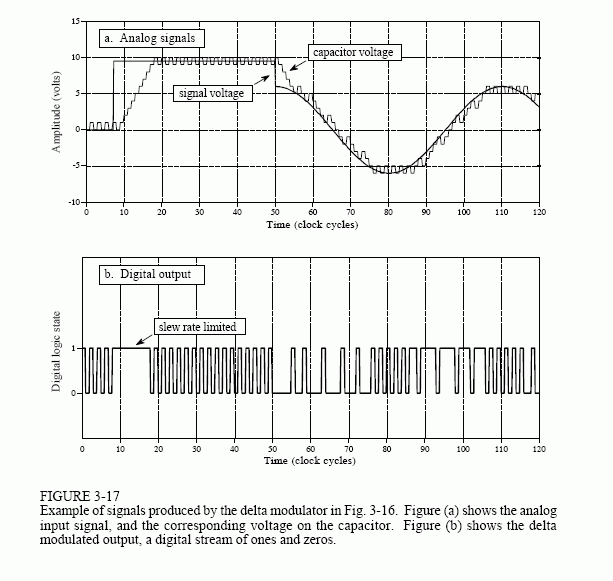
Figure 3-17 illustrates the signals produced by this circuit. At time equal zero, the analog input and the voltage on the capacitor both start with a voltage of zero. As shown in (a), the input signal suddenly increases to 9.5 volts on the eighth clock cycle. Since the input signal is now more positive than the voltage on the capacitor, the digital output changes to a one, as shown in (b). This results in the switch being connected to the positive charge injector, and the voltage on the capacitor increasing by a small amount on each clock cycle. Although an increment of 1 volt per clock cycle is shown in (a), this is only for illustration, and a value of 1 millivolt is more typical. This staircase increase in the capacitor voltage continues until it exceeds the voltage of the input signal. Here the system reached an equilibrium with the output oscillating between a digital one and zero, causing the voltage on the capacitor to oscillate between 9 volts and 10 volts. In this manner, the feedback of the circuit forces the capacitor voltage to track the voltage of the input signal. If the input signal changes very rapidly, the voltage on the capacitor changes at a constant rate until a match is obtained. This constant rate of change is called the slew rate, just as in other electronic devices such as op amps.
Now, consider the characteristics of the delta modulated output signal. If the analog input is increasing in value, the output signal will consist of more ones than zeros. Likewise, if the analog input is decreasing in value, the output will consist of more zeros than ones. If the analog input is constant, the digital output will alternate between zero and one with an equal number of each. Put in more general terms, the relative number of ones versus zeros is directly proportional to the slope (derivative) of the analog input.
This circuit is a cheap method of transforming an analog signal into a serial stream of ones and zeros for transmission or digital storage. An especially attractive feature is that all the bits have the same meaning, unlike the conventional serial format: start bit, LSB, ,MSB, stop bit. The circuit at the receiver is identical to the feedback portion of the transmitting circuit. Just as the voltage on the capacitor in the transmitting circuit follows the analog input, so does the voltage on the capacitor in the receiving circuit. That is, the capacitor voltage shown in (a) also represents how the reconstructed signal would appear.
A critical limitation of this circuit is the unavoidable tradeoff between (1) maximum slew rate, (2) quantization size, and (3) data rate. In particular, if the maximum slew rate and quantization size are adjusted to acceptable values for voice communication, the data rate ends up in the MHz range. This is too high to be of commercial value. For instance, conventional sampling of a voice signal requires only about 64,000 bits per second.
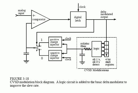
A solution to this problem is shown in Fig. 3-18, the Continuously Variable Slope Delta (CVSD) modulator, a technique implemented in the Motorola MC3518 family. In this approach, the clock rate and the quantization size are set to something acceptable, say 30 kHz, and 2000 levels. This results in a terrible slew rate, which you correct with additional circuitry. In operation, a shift resister continually looks at the last four bits that the system has produced. If the circuit is in a slew rate limited condition, the last four bits will be all ones (positive slope) or all zeros (negative slope). A logic circuit detects this situation and produces an analog signal that increase the level of charge produced by the charge injectors. This boosts the slew rate by increasing the size of the voltage steps being applied to the capacitor.
An analog filter is usually placed between the logic circuitry and the charge injectors. This allows the step size to depend on how long the circuit has been in a slew limited condition. As long as the circuit is slew limited, the step size keeps getting larger and larger. This is often called a syllabic filter, since its characteristics depend on the average length of the syllables making up speech. With proper optimization (from the chip manufacturer's
spec sheet, not your own work), data rates of 16 to 32 kHz produce acceptable quality speech. The continually changing step size makes the digital data difficult to understand, but fortunately, you don't need to. At the receiver, the analog signal is reconstructed by incorporating a syllabic filter that is identical to the one in the transmission circuit. If the two filters are matched, little distortion results from the CVSD modulation. CVSD is probably the easiest way to digitally transmit a voice signal.
While CVSD modulation is great for encoding voice signals, it cannot be used for general purpose analog-to-digital conversion. Even if you get around the fact that the digital data is related to the derivative of the input signal, the changing step size will confuse things beyond repair. In addition, the DC level of the analog signal is usually not captured in the digital data.
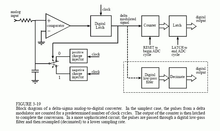
The delta-sigma converter, shown in Fig. 3-19, eliminates these problems by cleverly combining analog electronics with DSP algorithms. Notice that the voltage on the capacitor is now being compared with ground potential. The feedback loop has also been modified so that the voltage on the
capacitor is decreased when the circuit's output is a digital one, and increased when it is a digital zero. As the input signal increases and decreases in voltage, it tries to raise and lower the voltage on the capacitor. This change in voltage is detected by the comparator, resulting in the charge injectors producing a counteracting charge to keep the capacitor at zero volts.
If the input voltage is positive, the digital output will be composed of more ones than zeros. The excess number of ones being needed to generate the negative charge that cancels with the positive input signal. Likewise, if the input voltage is negative, the digital output will be composed of more zeros than ones, providing a net positive charge injection. If the input signal is equal to zero volts, an equal number of ones and zeros will be generated in the output, providing an overall charge injection of zero.
The relative number of ones and zeros in the output is now related to the level of the input voltage, not the slope as in the previous circuit. This is much simpler. For instance, you could form a 12 bit ADC by feeding the digital output into a counter, and counting the number of ones over 4096 clock cycles. A digital number of 4095 would correspond to the maximum positive input voltage. Likewise, digital number 0 would correspond to the maximum negative input voltage, and 2048 would correspond to an input voltage of zero. This also shows the origin of the name, delta-sigma: delta modulation followed by summation (sigma).
The ones and zeros produced by this type of delta modulator are very easy to transform back into an analog signal. All that is required is an analog low-pass filter, which might be as simple as a single RC network. The high
and low voltages corresponding to the digital ones and zeros average out to form the correct analog voltage. For example, suppose that the ones and zeros are represented by 5 volts and 0 volts, respectively. If 80% of the bits in the data stream are ones, and 20% are zeros, the output of the low-pass filter will be 4 volts.
This method of transforming the single bit data stream back into the original waveform is important for several reasons. First, it describes a slick way to replace the counter in the delta-sigma ADC circuit. Instead of simply counting the pulses from the delta modulator, the binary signal is passed through a digital low-pass filter, and then decimated to reduce the sampling rate. For example, this procedure might start by changing each of the ones and zeros in the digital stream into a 12 bit sample; ones become a value of 4095, while zeros become a value of 0. Using a digital low-pass filter on this signal produces a digitized version of the original waveform, just as an analog low-pass filter would form an analog recreation. Decimation then reduces the sampling rate by discarding most of the samples. This results in a digital signal that is equivalent to direct sampling of the original waveform.
This approach is used in many commercial ADC's for digitizing voice and other audio signals. An example is the National Semiconductor ADC16071, which provides 16 bit analog-to-digital conversion at sampling rates up to 192 kHz. At a sampling rate of 100 kHz, the delta modulator operates with a clock frequency of 6.4 MHz. The low-pass digital filter is a 246 point FIR, such as described in Chapter 16. This removes all frequencies in the digital data above 50 kHz, ? of the eventual sampling rate. Conceptually, this can be viewed as forming a digital signal at 6.4 MHz, with each sample represented by 16 bits. The signal is then decimated from 6.4 MHz to 100 kHz, accomplished by deleting every 63 out of 64 samples. In actual operation, much more goes on inside of this device than described by this simple discussion.
Delta-sigma converters can also be used for digital-to-analog conversion of voice and audio signals. The digital signal is retrieved from memory, and converted into a delta modulated stream of ones and zeros. As mentioned above, this single bit signal can easily be changed into the reconstructed analog signal with a simple low-pass analog filter. As with the antialias filter, usually only a single RC network is required. This is because the majority of the filtration is handled by the high-performance digital filters.
Delta-sigma ADC's have several quirks that limit their use to specific applications. For example, it is difficult to multiplex their inputs. When the input is switched from one signal to another, proper operation is not established until the digital filter can clear itself of data from the previous signal. Delta-sigma converters are also limited in another respect: you don't know exactly when each sample was taken. Each acquired sample is a composite of the one bit information taken over a segment of the input signal. This is not a problem for signals encoded in the frequency domain, such as audio, but it is a significant limitation for time domain encoded signals. To understand the shape of a signal's waveform, you often need to know the precise instant each sample was taken. Lastly, most of these devices are specifically designed for audio applications, and their performance specifications are quoted accordingly. For example, a 16 bit ADC used for voice signals does not necessarily mean that each sample has 16 bits of precision. Much more likely, the manufacturer is stating that voice signals can be digitized to 16 bits of dynamic range. Don't expect to get a full 16 bits of useful information from this device for general purpose data acquisition.
While these explanations and examples provide an introduction to single bit ADC and DAC, it must be emphasized that they are simplified descriptions of sophisticated DSP and integrated circuit technology. You wouldn't expect the manufacturer to tell their competitors all the internal workings of their chips, so don't expect them to tell you.