The Scientist and Engineer's Guide to
Digital Signal Processing
By Steven W. Smith, Ph.D.
Book Search

Table of contents
- 1: The Breadth and Depth of DSP
- 2: Statistics, Probability and Noise
- 3: ADC and DAC
- 4: DSP Software
- 5: Linear Systems
- 6: Convolution
- 7: Properties of Convolution
- 8: The Discrete Fourier Transform
- 9: Applications of the DFT
- 10: Fourier Transform Properties
- 11: Fourier Transform Pairs
- 12: The Fast Fourier Transform
- 13: Continuous Signal Processing
- 14: Introduction to Digital Filters
- 15: Moving Average Filters
- 16: Windowed-Sinc Filters
- 17: Custom Filters
- 18: FFT Convolution
- 19: Recursive Filters
- 20: Chebyshev Filters
- 21: Filter Comparison
- 22: Audio Processing
- 23: Image Formation & Display
- 24: Linear Image Processing
- 25: Special Imaging Techniques
- 26: Neural Networks (and more!)
- 27: Data Compression
- 28: Digital Signal Processors
- 29: Getting Started with DSPs
- 30: Complex Numbers
- 31: The Complex Fourier Transform
- 32: The Laplace Transform
- 33: The z-Transform
- 34: Explaining Benford's Law
How to order your own hardcover copy
Wouldn't you rather have a bound book instead of 640 loose pages?Your laser printer will thank you!
Order from Amazon.com.
Chapter 28: Digital Signal Processors
One of the biggest bottlenecks in executing DSP algorithms is transferring information to and from memory. This includes data, such as samples from the input signal and the filter coefficients, as well as program instructions, the binary codes that go into the program sequencer. For example, suppose we need to multiply two numbers that reside somewhere in memory. To do this, we must fetch three binary values from memory, the numbers to be multiplied, plus the program instruction describing what to do.
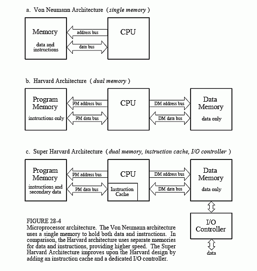
Figure 28-4a shows how this seemingly simple task is done in a traditional microprocessor. This is often called a Von Neumann architecture, after the brilliant American mathematician John Von Neumann (1903-1957). Von Neumann guided the mathematics of many important discoveries of the early twentieth century. His many achievements include: developing the concept of a stored program computer, formalizing the mathematics of quantum mechanics, and work on the atomic bomb. If it was new and exciting, Von Neumann was there!
As shown in (a), a Von Neumann architecture contains a single memory and a single bus for transferring data into and out of the central processing unit (CPU). Multiplying two numbers requires at least three clock cycles, one to transfer each of the three numbers over the bus from the memory to the CPU. We don't count the time to transfer the result back to memory, because we assume that it remains in the CPU for additional manipulation (such as the sum of products in an FIR filter). The Von Neumann design is quite satisfactory when you are content to execute all of the required tasks in serial. In fact, most computers today are of the Von Neumann design. We only need other architectures when very fast processing is required, and we are willing to pay the price of increased complexity.
This leads us to the Harvard architecture, shown in (b). This is named for the work done at Harvard University in the 1940s under the leadership of Howard Aiken (1900-1973). As shown in this illustration, Aiken insisted on separate memories for data and program instructions, with separate buses for each. Since the buses operate independently, program instructions and data can be fetched at the same time, improving the speed over the single bus design. Most present day DSPs use this dual bus architecture.
Figure (c) illustrates the next level of sophistication, the Super Harvard Architecture. This term was coined by Analog Devices to describe the internal operation of their ADSP-2106x and new ADSP-211xx families of Digital Signal Processors. These are called SHARC® DSPs, a contraction of the longer term, Super Harvard ARChitecture. The idea is to build upon the Harvard architecture by adding features to improve the throughput. While the SHARC DSPs are optimized in dozens of ways, two areas are important enough to be included in Fig. 28-4c: an instruction cache, and an I/O controller.
First, let's look at how the instruction cache improves the performance of the Harvard architecture. A handicap of the basic Harvard design is that the data memory bus is busier than the program memory bus. When two numbers are multiplied, two binary values (the numbers) must be passed over the data memory bus, while only one binary value (the program instruction) is passed over the program memory bus. To improve upon this situation, we start by relocating part of the "data" to program memory. For instance, we might place the filter coefficients in program memory, while keeping the input signal in data memory. (This relocated data is called "secondary data" in the illustration). At first glance, this doesn't seem to help the situation; now we must transfer one value over the data memory bus (the input signal sample), but two values over the program memory bus (the program instruction and the coefficient). In fact, if we were executing random instructions, this situation would be no better at all.
However, DSP algorithms generally spend most of their execution time in loops, such as instructions 6-12 of Table 28-1. This means that the same set of program instructions will continually pass from program memory to the CPU. The Super Harvard architecture takes advantage of this situation by including an instruction cache in the CPU. This is a small memory that contains about 32 of the most recent program instructions. The first time through a loop, the program instructions must be passed over the program memory bus. This results in slower operation because of the conflict with the coefficients that must also be fetched along this path. However, on additional executions of the loop, the program instructions can be pulled from the instruction cache. This means that all of the memory to CPU information transfers can be accomplished in a single cycle: the sample from the input signal comes over the data memory bus, the coefficient comes over the program memory bus, and the program instruction comes from the instruction cache. In the jargon of the field, this efficient transfer of data is called a high memory-access bandwidth.
Figure 28-5 presents a more detailed view of the SHARC architecture, showing the I/O controller connected to data memory. This is how the signals enter and exit the system. For instance, the SHARC DSPs provides both serial and parallel communications ports. These are extremely high speed connections. For example, at a 40 MHz clock speed, there are two serial ports that operate at 40 Mbits/second each, while six parallel ports each provide a 40 Mbytes/second data transfer. When all six parallel ports are used together, the data transfer rate is an incredible 240 Mbytes/second.
This is fast enough to transfer the entire text of this book in only 2 milliseconds! Just as important, dedicated hardware allows these data streams to be transferred directly into memory (Direct Memory Access, or DMA), without having to pass through the CPU's registers. In other words, tasks 1 & 14 on our list happen independently and simultaneously with the other tasks; no cycles are stolen from the CPU. The main buses (program memory bus and data memory bus) are also accessible from outside the chip, providing an additional interface to off-chip memory and peripherals. This allows the SHARC DSPs to use a four Gigaword (16 Gbyte) memory, accessible at 40 Mwords/second (160 Mbytes/second), for 32 bit data. Wow!
This type of high speed I/O is a key characteristic of DSPs. The overriding goal is to move the data in, perform the math, and move the data out before the next sample is available. Everything else is secondary. Some DSPs have on-board analog-to-digital and digital-to-analog converters, a feature called mixed signal. However, all DSPs can interface with external converters through serial or parallel ports.
Now let's look inside the CPU. At the top of the diagram are two blocks labeled Data Address Generator (DAG), one for each of the two memories. These control the addresses sent to the program and data memories, specifying where the information is to be read from or written to. In simpler microprocessors this task is handled as an inherent part of the program sequencer, and is quite transparent to the programmer. However, DSPs are designed to operate with circular buffers, and benefit from the extra hardware to manage them efficiently. This avoids needing to use precious CPU clock cycles to keep track of how the data are stored. For instance, in the SHARC DSPs, each of the two DAGs can control eight circular buffers. This means that each DAG holds 32 variables (4 per buffer), plus the required logic.
Why so many circular buffers? Some DSP algorithms are best carried out in stages. For instance, IIR filters are more stable if implemented as a cascade of biquads (a stage containing two poles and up to two zeros). Multiple stages require multiple circular buffers for the fastest operation. The DAGs in the SHARC DSPs are also designed to efficiently carry out the Fast Fourier transform. In this mode, the DAGs are configured to generate bit-reversed addresses into the circular buffers, a necessary part of the FFT algorithm. In addition, an abundance of circular buffers greatly simplifies DSP code generation- both for the human programmer as well as high-level language compilers, such as C.
The data register section of the CPU is used in the same way as in traditional microprocessors. In the ADSP-2106x SHARC DSPs, there are 16 general purpose registers of 40 bits each. These can hold intermediate calculations, prepare data for the math processor, serve as a buffer for data transfer, hold flags for program control, and so on. If needed, these registers can also be used to control loops and counters; however, the SHARC DSPs have extra hardware registers to carry out many of these functions.
The math processing is broken into three sections, a multiplier, an arithmetic logic unit (ALU), and a barrel shifter. The multiplier takes the values from two registers, multiplies them, and places the result into another register. The ALU performs addition, subtraction, absolute value, logical operations (AND, OR, XOR, NOT), conversion between fixed and floating point formats, and similar functions. Elementary binary operations are carried out by the barrel shifter, such as shifting, rotating, extracting and depositing segments, and so on. A powerful feature of the SHARC family is that the multiplier and the ALU can be accessed in parallel. In a single clock cycle, data from registers 0-7 can be passed to the multiplier, data from registers 8-15 can be passed to the ALU, and the two results returned to any of the 16 registers.
There are also many important features of the SHARC family architecture that aren't shown in this simplified illustration. For instance, an 80 bit accumulator is built into the multiplier to reduce the round-off error associated with multiple fixed-point math operations. Another interesting
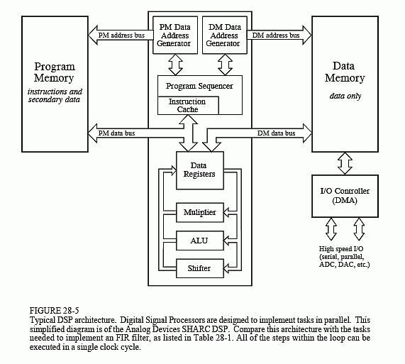
feature is the use of shadow registers for all the CPU's key registers. These are duplicate registers that can be switched with their counterparts in a single clock cycle. They are used for fast context switching, the ability to handle interrupts quickly. When an interrupt occurs in traditional microprocessors, all the internal data must be saved before the interrupt can be handled. This usually involves pushing all of the occupied registers onto the stack, one at a time. In comparison, an interrupt in the SHARC family is handled by moving the internal data into the shadow registers in a single clock cycle. When the interrupt routine is completed, the registers are just as quickly restored. This feature allows step 4 on our list (managing the sample-ready interrupt) to be handled very quickly and efficiently.
Now we come to the critical performance of the architecture, how many of the operations within the loop (steps 6-12 of Table 28-1) can be carried out at the same time. Because of its highly parallel nature, the SHARC DSP can simultaneously carry out all of these tasks. Specifically, within a single clock cycle, it can perform a multiply (step 11), an addition (step 12), two data moves (steps 7 and 9), update two circular buffer pointers (steps 8 and 10), and control the loop (step 6). There will be extra clock cycles associated with beginning and ending the loop (steps 3, 4, 5 and 13, plus moving initial values into place); however, these tasks are also handled very efficiently. If the loop is executed more than a few times, this overhead will be negligible. As an example, suppose you write an efficient FIR filter program using 100 coefficients. You can expect it to require about 105 to 110 clock cycles per sample to execute (i.e., 100 coefficient loops plus overhead). This is very impressive; a traditional microprocessor requires many thousands of clock cycles for this algorithm.